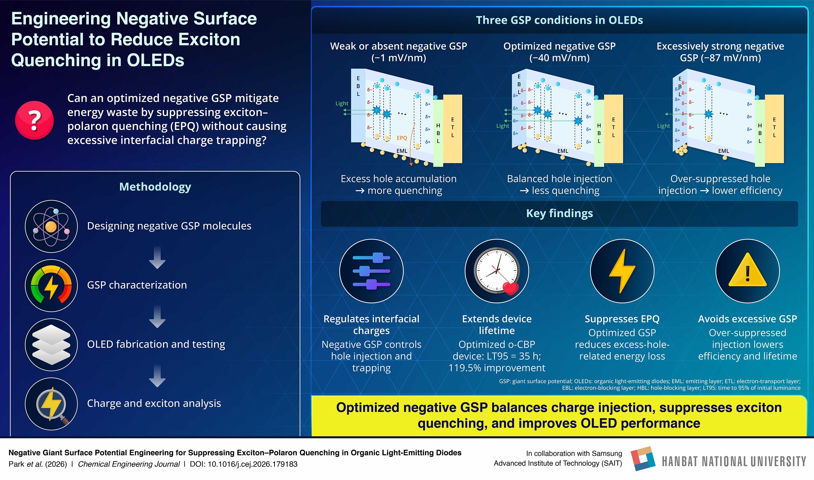
A research team led by Professor Jae-Hyun Lee of the Department of Creative Convergence Engineering at Hanbat National University, working with Dr Jong Soo Kim of the Samsung Advanced Institute of Technology, placed thin electron-blocking layers between the hole-transport and light-emitting layers of organic light-emitting diodes, according to Hanbat National University. The layer was intended to adjust the local electrical environment where excess positive charges, or holes, collect and interfere with light-producing excitons, a loss process the researchers call exciton–polaron quenching.
35 hours against 29
The team compared three materials whose negative giant surface potential measured −1, −40 and −87 millivolts per nanometer, using electrical measurements, impedance spectroscopy, transient electroluminescence and photoluminescence to track charge movement and light loss. The o-CBP layer, at −40 millivolts per nanometer, gave the best balance in the tested devices: an LT95 lifetime of 35 hours against about 29 hours for the reference, roughly 20% longer, where LT95 is the time for luminance to fall to 95% of its starting level under the study's test conditions. The strongest material, PhCzCz-PhTPS at −87 millivolts per nanometer, held holes too tightly at the interface and restricted charge injection, cutting current and the formation of light-emitting excitons, which lowered efficiency and shortened lifetime.
Published in October
The paper was made available online on July 7, 2026, and appeared in Volume 545 of the Chemical Engineering Journal on October 1, 2026. Professor Lee said the key was to control the interface potential between layers rather than to use the material with the strongest surface potential, and that an intermediate negative value can cut energy loss while preserving the charge flow needed for emission.
Laboratory conditions only
The university said the experiments tested the diodes under laboratory conditions and do not establish longer battery life, reduced burn-in or better image quality in commercial products. It said further testing across device designs and operating conditions is needed to show how widely the approach can improve display performance, and that the same principle of tuning negative surface potential to surrounding layers may inform other organic electronics where charge build-up at interfaces adds to energy loss.